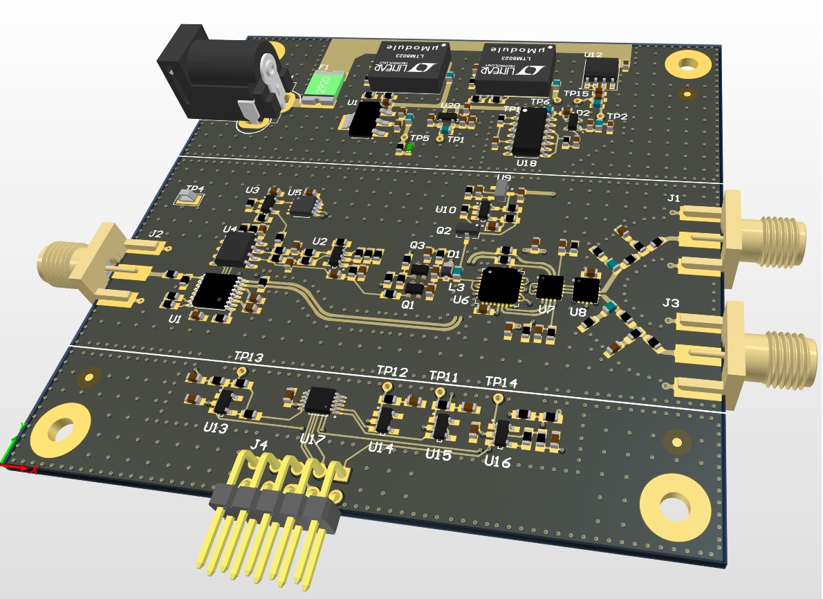
High-Speed Embedded Edge Vision & Multi-Band RF Integration
Engineering an Ultra-Compact Wearable Platform for Mission-Critical Hardware Applications
1. Protocol & Interface Matrix
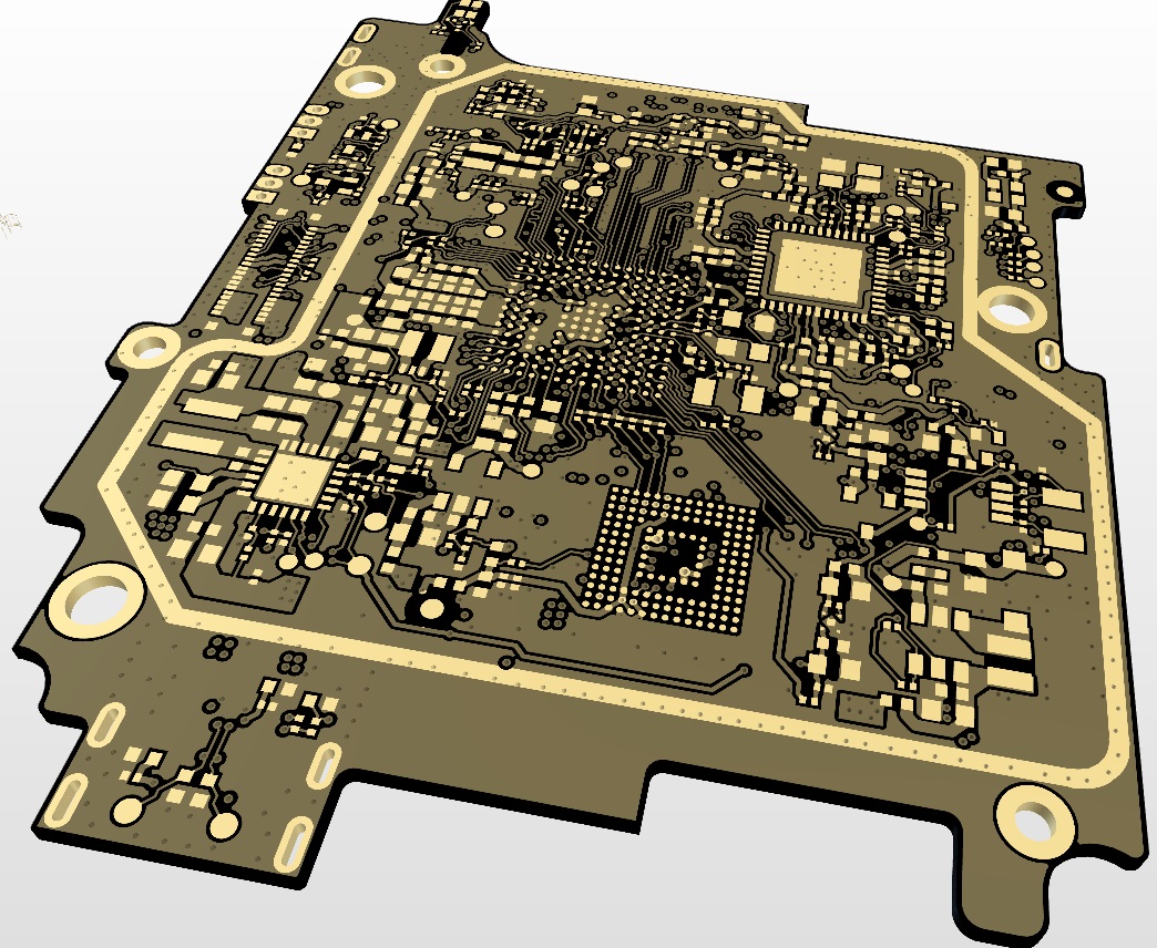
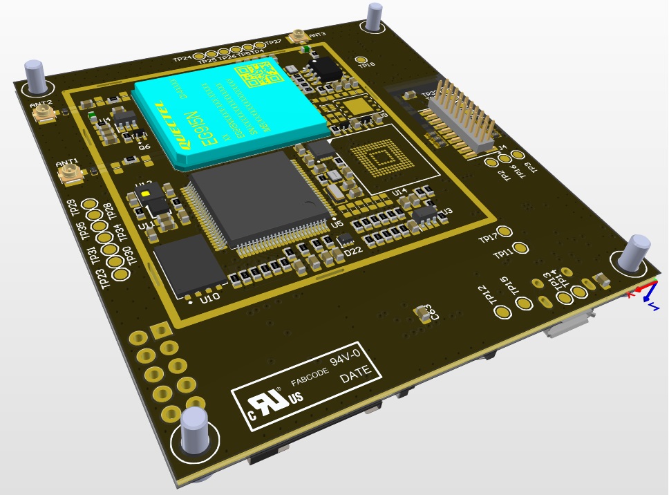
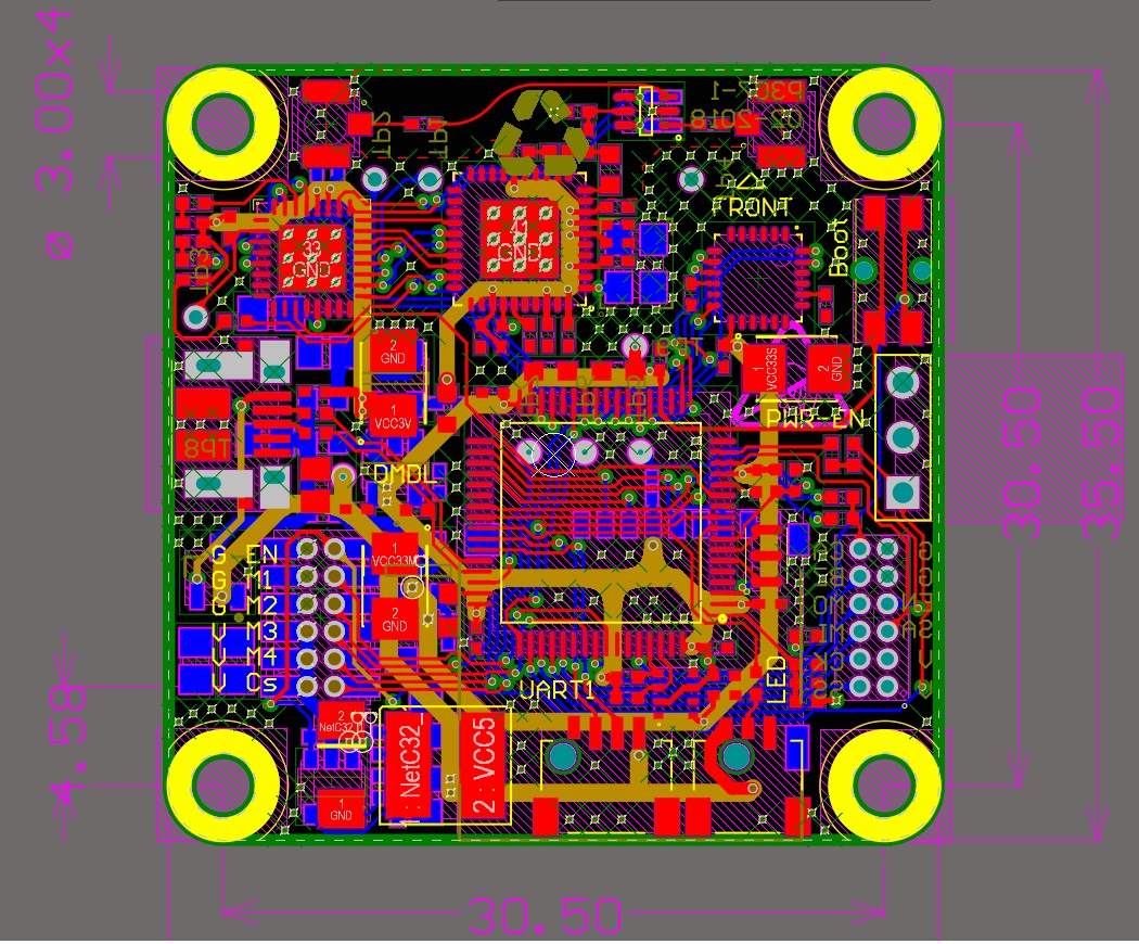
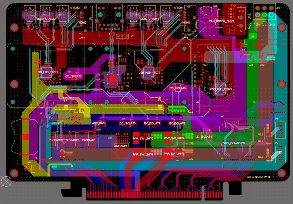
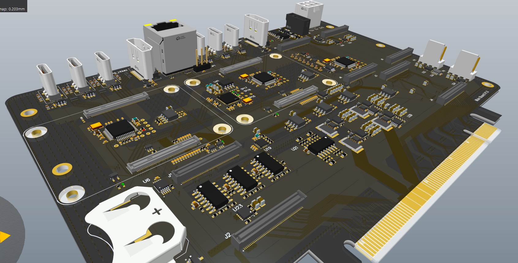
Designing a multi-functional, ultra-compact smart camera system requires orchestrating several high-speed digital, RF, and low-speed control protocols on a single HDI stackup:
High-Speed Digital Memory & Bus Protocols
- DDR4 / DDR3 Memory: DDR4-2400/3200 (and legacy DDR3L) running SSTL_12 / SSTL_15 signaling with strict length-matching, write-leveling, and address/control/command skew budgets.
- USB 3.1 Gen 2 / Gen 1: SuperSpeed/SuperSpeed+ differential signaling at up to 10 Gbps utilizing NRZ / 128b/130b encoding over impedance-matched 90 Ω differential pairs.
- SerDes (Sensor Extension): FPD-Link III / GMSL2 / V-by-One high-speed serializer/deserializer links over coaxial or STP cabling, transmitting multi-gigabit video and bi-directional backchannel data.
- Camera Interfaces: MIPI CSI-2 (D-PHY v1.2/v2.0 or C-PHY) delivering multi-lane raw sensor data directly to the host SoC/FPGA.
RF, Wireless & Control Protocols
- 5G Sub-6 GHz & mmWave: PCIe Gen 3/4 or USB 3.1 interface to 5G NR modem modules operating across frequency bands with MIMO antenna structures.
- Wi-Fi 6/6E & Bluetooth 5.2/5.3: Dual-band/tri-band 2.4 GHz, 5 GHz, and 6 GHz Wi-Fi (IEEE 802.11ax) paired with BT LE co-existence RF paths.
- Low-Speed Control Interfaces: I2C / I3C / SPI for sensor control, PMIC configuration, and register programming; UART & GPIO for synchronization triggers.
2. Key Engineering & Co-Existence Challenges
A. Mixed-Signal Crosstalk & SI/PI Integration
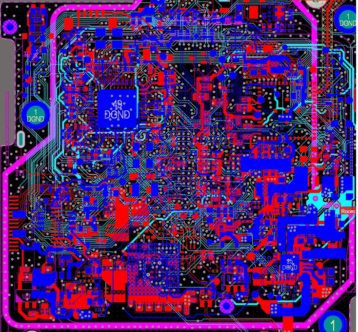
Route high-speed DDR4 byte lanes, 10 Gbps USB 3.1 lines, and multi-gigabit SerDes signals alongside sensitive 5G/Wi-Fi RF traces within a restricted board outline. Simultaneous switching noise (SSN) from memory buses and high-current power rails can easily couple into unshielded RF front-ends, degrading receiver sensitivity (desense).
B. Power Integrity (PI) & Signal Integrity (SI) Co-Optimization
Ultra-compact form factors prohibit large bulk capacitors. Maintaining clean Power Delivery Networks (PDN) with sub-10 mΩ target impedance up to multi-gigahertz frequencies demands advanced planar capacitance stackups, buried microvias, and low-ESR ceramic decoupling arrays placed directly underneath BGA components.
C. FCC Certification & Signal Emissivity (SE) Compliance
To pass FCC Class B and RED radiated emission testing, high-speed differential pairs must maintain strict skew symmetry to eliminate common-mode radiation. Comprehensive ground shielding fences, ground via-stitching around high-speed traces, and localized RF cans are mandated to prevent harmonic leaks from DDR clock trees and USB 3.1 data lines into 5G/Wi-Fi bands.
D. Thermal Stability & Li-Ion Battery Longevity
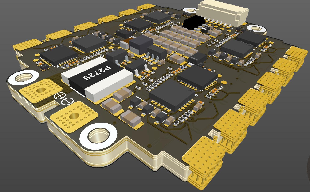
Packing a high-throughput camera ISP, DDR4 memory, SerDes bridge, and 5G transceiver into a wearable enclosure generates concentrated thermal loads (5–10W+ in a miniature footprint). Elevated operational temperatures accelerate Li-ion battery degradation (capacity fade and internal impedance growth). Thermal mitigation requires strategic copper heat-spreading planes, thermal microvia arrays, dynamic frequency scaling, and thermally isolated battery chambers to protect cell health over thousands of charge cycles.
The Vostek Inc. Advantage
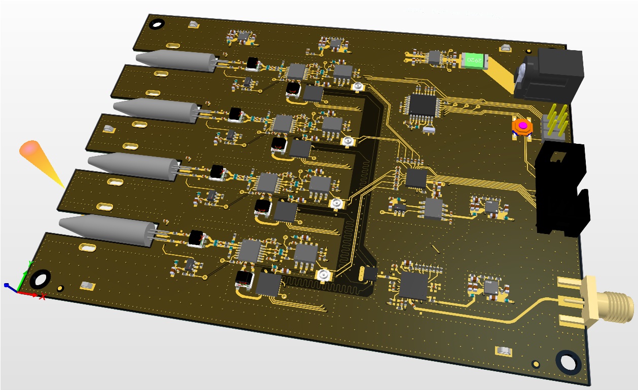
At Vostek Inc., our team of senior hardware engineers and analytical specialists excels in conquering the physical limits of high-density HDI design. Utilizing state-of-the-art 3D EM full-wave field solvers, signal/power integrity (SI/PI) simulations, and thermal-mechanical modeling, Vostek turns complex multi-protocol architectures—such as 12-layer microvia wearable boards with 5G, DDR4, MIPI CSI-2, and SerDes—into production-ready, FCC-compliant hardware. From sub-nanosecond pulse generation and 5.8 GHz RF optimization to ruggedized wearable form factors, Vostek Inc. provides turnkey hardware excellence for mission-critical applications.